
Samsung plans to leapfrog TSMC and Intel to become the first major foundry to get a version of gate all-around transistors in production.
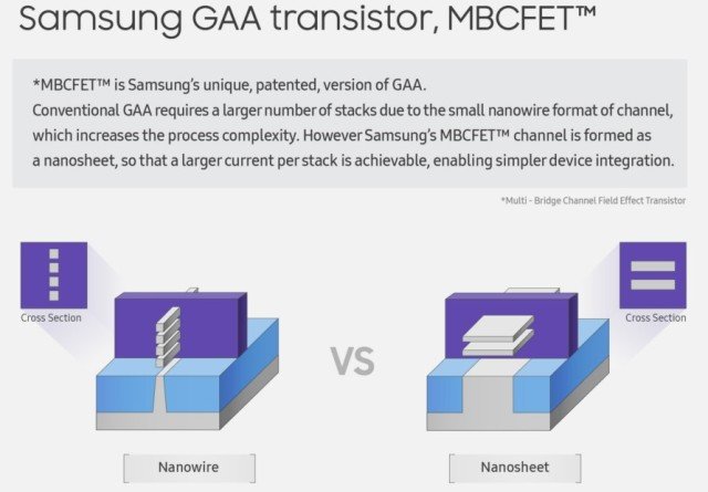
Samsung Foundry recently held its Foundry Forum where it revealed some details of its semiconductor process roadmaps and fab expansion. Samsung is being most aggressive pursuing the next generation of transistor technology, with plans to reach mass production ahead of TSMC and Intel. Samsung’s 3-nanometer process will use the gate-all-around (GAA) transistor structure, which the foundry calls MBCFET (Multi-bridge channel FET) and will be in production first half of 2022. TSMC will wait another generation until its N2 process to deliver GAA some time in 2023.
Intel will bring its version of GAA, called RibbonFET, into production in its 20A process, likely in mid-2024. While Samsung is being the most aggressive on this technology, TSMC will deliver its 3-nanometer node earlier in 2022 using the more conservative approach by extending the life of FinFET designs. Intel will also use its “Enhanced SuperFin” transistors for the Intel 4 node in 2022, and the Intel 3 node in 2023. All these new nodes, both FinFET and GAA, are using extreme ultraviolet (EUV) lithography. It should also be noted, that neither Samsung nor TSMC has decided to follow Intel and rescale the node names from nanometers to Angstroms, at least not yet.
The first Samsung GAA node is 3GAE, in mass production by end of 2022, followed by the 3GAP node by the end of 2023. The 2GAP node will not make it into mass production until 2025. Samsung executives said at a press conference before the Forum that its new MBCFET technology is more expensive to manufacture, but it will “strive” to continue to lower the cost per transistor. The 3nm MBCFET node will allow up to 35% decrease in area, 30% higher performance or 50% lower power consumption compared to its 5nm process.
10/17-19 EAC