
Today, the trend common to every electronics sector is the search for maximum efficiency. Energy harvesting techniques can not only minimize—if not eliminate—maintenance interventions, but it can also reduce current consumption and minimization of power losses, enabling more efficient use of energy resources and the fulfillment of requirements imposed by recent global regulations.
In the specific case of ultra-low power applications, energy efficiency assumes a fundamental importance for the feasibility of the device. This applies to IoT devices, whose number is expected to exceed 40 billion of connected units in 2025, according to IDC’s Worldwide Global DataSphere IoT Device and Data Forecast. In many cases, IoT devices are powered by rechargeable batteries that users must replace periodically.
By capturing and converting different forms of energy available in the environment, such as solar or wind power, it is possible to obtain the electrical energy required to recharge IoT device batteries. Other forms of usable energy are radio frequency (RF) signals, mechanical or kinetic energy, solar power, and thermal energy.
It is also worth noting that energy harvesting is an excellent method for addressing the issue of climate change and global warming because it recycles outside energy that would otherwise be lost.
Energy harvesting sources
An overview of the most common energy harvesting sources is as follows:
Thermal energy — Thermal energy is found everywhere in the environment around us as temperature variations and heat flows. The heat produced by engine waste, geothermal heat from the soil, heat from cooling water in steelworks, and other industrial operations are typical examples. You can transform thermal energy into electrical energy using a thermoelectric generator and some electronics. The electrical energy can then be saved in a storage device. The thermoelectric generator (TEG) works on the basic tenet that heat flux (temperature difference) can be converted into electrical energy. TEGs are perfect for low-power embedded devices because they typically have very small sizes and no moving partsRF energy — RF energy harvesters can transform RF energy into electrical energy. Today, RF energy produced by radio waves, GSM, LTE and other technologies is all around us. Any business, residential or industrial location has all these signals. Recovery of the power transmitted by public telecommunications services, such as TV, radio broadcasting or even mobile communications, is the challenge often experienced during research and development of these technologies.Solar radiation — Solar energy is everywhere and can be easily exploited through photovoltaic panels or sensors specifically developed for energy harvesting.Kinetic energy — Piezoelectric crystals produce low voltages by converting mechanical motion. In this scenario, the kinetic energy of a magnetized object can help produce electrical energy. Different activities, such as walking, moving around, or the usage of micro-turbines under clothing to take advantage of air circulation, can cause mechanical motion.Energy harvesting circuit design
Designing and implementing an energy harvesting circuit is not a simple task, considering that the power obtained with this technique is very low (milliwatts or microwatts). Therefore, components and design solutions that can make the most of the available energy, minimize losses and maximize efficiency are needed.
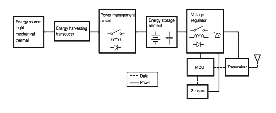
A typical energy harvesting scheme is composed of an ambient energy source, energy transducer, power management unit, energy storage element, voltage regulator and electrical load, as shown in Figure 1.
Some circuit solutions related to energy harvesting (EH) applications are as follows:
EH circuit for converting RF and thermal energy into electrical energy.EH circuit for the conversion of light energy into electrical energy.Harvesting of RF and thermal energy
The BQ25570 IC, which can extract microwatts to milliwatts from thermoelectric generators, can be used for thermal energy harvesting. Additionally, it incorporates a power management system that uses multiple circuits to raise voltages, all while preventing overcharging or explosion of the battery.
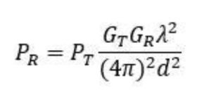
Regarding the assessment of the power level at the receiving antenna, we can use the well-known Friis transmission equation below, where: PT = transmitted power, PR = received power, GT = transmitter antenna gain, GR = receiver antenna gain, λ = wavelength, and d = distance between transmitter and receiver.
By combining both RF and thermal sensors, a low-power wearable device can receive enough energy to enable self-powering. The resulting block diagram is shown in Figure 2.
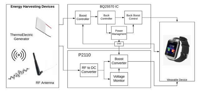
As an example, we will utilize the P2110 IC, together with its RF antenna and front end, for RF harvesting. It is set to the 902 to 928 Mhz range of frequencies.
The procedure begins when the thermoelectric generator’s plates have a sufficient temperature difference between them to produce a voltage on their terminals. The BQ25570 IC will extract the power, which will vary in size according on the temperature differential, from microwatts to milliwatts. The voltage will then be increased to 3.3 V with 93% efficiency thanks to the built-in boost converter.
The P2110 RF harvester will also transform RF energy into electrical energy. The antenna will receive the RF power, which will then convert to a DC source using its built-in impedance matching circuit. When the device uses less current than that produced by the harvester circuit, a capacitor is placed at the output to store power. Both abilities will then be united and made operational simultaneously. The system continues to function even if one of the harvesting sources is weak because the other source will continue to supply electricity.
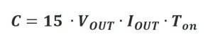
The selected capacitor shall feature low ESR (less than 200 mΩ) and low leakage current (less than 1 μA at 1.2V). Moreover, its value can be calculated according to the following formula, where: VOUT = Output voltage of the P2110, Ton = IC turn-on time, and IOUT = Average output current from the P2110.
The IC’s RF input pin may accept any common antenna. A 50-Ohm antenna is employed for this project because it is typical for most RF equipment to use one for impedance matching. Antennas of various types can be connected to the P2110.
Extra attention must be given while designing the PCB because RF is highly susceptible to noise and EMI interference. The trace antenna’s impedance matching is of utmost importance. The length of the RF trace must be kept to a rigorous maximum of 50 Ohms. The GND pins should be connected to the board ground using vias. The IC must also be near all resistors and capacitors.
In addition, PCB traces for the high current tracks should be short and wide. The return route should be as brief as feasible from the ground. The proximity of the store and bypass capacitors should equal that of the IC pad. Avoid placing any vias in the capacitor’s route.
Solar radiation harvesting
Solar radiation harvesting uses a tiny photodiode, driven by a power harvesting IC, to provide low-power applications with power. The output of the photodiode is used to charge a supercapacitor, whereas a buck converter is used to provide a 3.3 V regulated voltage.
The tiny BPW34 solar cell serves as the major element of this circuit (see Figure 3), converting solar energy into electrical energy. The BQ25504 IC is powered by the solar cell’s output, which is close to 300mV.
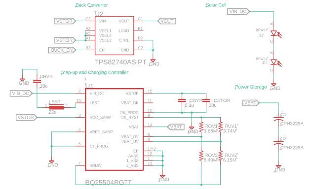
To start the IC, we will need to connect at least two solar cells in series, as 300 mV is insufficient. But even so, adding parallel solar cells can be used to speed up the IC’s startup time. It will charge the two CPH3225A (0.011F supercapacitors) connected in series by this step-up converter IC.
The highest output voltage of the IC, which is 5.25 V, is the only value that the supercapacitors would charge above. The supercapacitors will be discharged from 5 V to 3.3 V by the buck converter, which will also discharge the IC. The resistors linked to the harvester IC regulate both the overvoltage and undervoltage circumstances.
Because supercapacitors have their own restrictions, this module is appropriate for low-power applications. Under ideal circumstances, two CPH3255A can store a total of 12.74uWh (45.85mJ), or 3.86uAh at 3.3 V. Given that the CPH3225A has an internal resistance of 160 Ohms, the module can only supply a maximum of 10 mA, which is sufficient for even the most demanding uses.
For high currents like 10uA, the project’s efficiency is good. For lower currents, the buck converter will negatively impact the efficiency. At 10uA, the theoretically measured efficiency is 90%, but at smaller currents, such as 1uA, it drops to approximately 60%.
Like the previous project, the CBYP capacitor should have low leakage, while the CSTOR capacitor should have a low ESR, as its value affects the cold start efficiency and time.
This article was originally published on EE Times.
Maurizio Di Paolo Emilio is Editor in Chief of Power Electronics News and EEWeb, and an EE Times correspondent. He holds a Ph.D in physics and is a telecommunications engineer. He has worked on projects concerning gravitational waves research, designing a thermal compensation system (TCS) and data acquisition and control systems, and on others about x-ray microbeams in collaboration with Columbia University. TCS was applied to the Virgo and LIGO experiments, which detected gravitational waves for the first time and earned the Nobel Prize in 2017. He previously edited Firmware and Elettronica Open Source. He joined AspenCore in 2019.